
Penn had used Cadence IC tools for some years before the Cadence
University Program was developed, and has been an enthusiastic member
of the program since it was announced.
Cadence Design Systems has a wide variety of ways to interact with its
industrial customers (web sites, application engineers, and other
support personnel). The support for University Program members is
organized somewhat differently so that all questions from students or
staff flow through one of the Penn designated technical liaisons - see
the bottom of the page. It is possible for students to request help
from the appropriate liaison and he / she must then choose how to
address the particular problem using the tools available to him /
her. However, there is also more direct access to various other
Cadence programs, including the Cadence Designer's Network. In
addition, the University Program (see link above) itself has links to
many useful materials at other universities.
Cadence also runs an annual conference, CNDLive, (CDNLive) for industrial
users of their products which is also open to university members. No
one from Penn was able to attend the most recent sessions, but the
2005 conference provided useful insights into the tool suites and
development plans. Anyone interested in attending next year's
conference should check with the Cadence web site or with Josh Klien
or Paul Keener for particulars.
Through the Cadence University Program, Penn students and researchers
have access to and use of very powerful design and verification tools
for bipolar and CMOS integrated circuits, complex printed circuit
boards, and FPGAs. The tools are available to the entire Penn
community, but the licensing and primary contacts with Cadence Design
Systems are through the High Energy Physics group of the Department of
Physics and Astronomy.
Cadence tools are used for classes in Electrical and System
Engineering - see below - and are also used for Senior projects and
graduate level research projects in ESE. The tools are also used by
undergraduate and graduate students plus postdocs, faculty, and staff
for research projects in High Energy Physics, Astrophysics, and
Medical Physics. The various areas of use and some examples of
projects are listed below.
Departmental Use:
Electrical and Systems Engineering
The IC tools are used by the Department of Electrical and Systems
Engineering ESE570 / 319 course DIGITAL INTEGRATED CIRCUITS AND VLSI
FUNDAMENTALS taught by Prof. T. Khanna (ESE 570 web site is
http://www.seas.upenn.edu/~ese570/ this includes an on-line
Cadence tutorial developed by one of the students). The IC and RF
tools are also used in ESE 572 / 419 ANALOG INTEGRATED CIRCUIT DESIGN
and ESE 680 INTEGRATED COMMUNICATION SYSTEMS both taught by
Prof. Firooz Aflatouni - the ESE 572/680 web site is under
construction. Students and TAs in ESE 578 RF INTEGRATED CIRCUITS
taught by Prof. Tom Farmer also use the IC and RF tools. The Senior
Design Course EE441/442 is a project oriented course and a number of
student teams do IC design projects each year using the IC tools. In
addition, graduate research, independent projects (ESE899/999), Master
and PhD thesis (ESE990/995) are often based on use of the IC and RF
tools and hardware design language (HDL) tools. For all ESE use, the
primary technical contact is Firooz Aflatouni (firooz@seas.upenn.edu).
The IC and board level tools are used by both the research staff and by graduate (PHYS 899/999) and undergraduate students working on research projects in particle physics and astrophysics.
High Energy Physics
The primary particle physics research projects using Cadence tools are:
ATLAS
LSST
SNO+
In addition there is a joint project with the Hospital of the
University of Pennsylvania in medical imaging (PET and related
topics) using some of the board level tools. A board for doing
fast (~200 ps) timing on PET signals is now in use on the LaPET
scanner in DRL - the board is 12" x 18" and has over
12,000 parts - mostly 1.0 x 0.5 mm resistors, a joy to stuff and
test. An entirely new readout system for this research scanner is
under design now using high speed waveform recording devices
developed at the Paul Scheerer Institute in Switzerland.
The
Instrumentation/Engineering Group of the High Energy Physics
research effort is the primary contact with CDS. The technical
liaisons for HEP are Paul Keener (keener@hep.upenn.edu) for
installation and configuration and Nandor Dressnandt
(nandor@hep.upenn.edu) for IC and PCB tool issues.
Cadence tools are used by students and research staff in the High
Energy Physics group of the Physics and Astronomy Department to
advance the design and construction of large research
instruments. The most newsworthy of the projects we are involved
in is probably the Large Hadron Collider (LHC) at CERN, Geneva,
Switzerland – the most powerful accelerator ever built. Penn has
been heavily involved in the design and construction of the ATLAS
detector – especially the Transition Radiation Tracker (TRT). The
picture below is of an energetic cosmic ray showering in the two
meter diameter TRT during a commissioning run in 2009. Collision
data (the TRT can take events at 40MHz) is now being reported at
conferences and in publications.
With the TRT installed and operating, we have turned our focus to a tracker upgrade project, the InnerTracker (ITk). ITk is an all silicon tracker consisting of a pixel detector in the inner layers and a strip detector in the outter layers. With a strong contingent of phyics and electrical engineering students, we have participated in the design and verification of all three front-end ASICs for the ITk strip detector, with Penn being the lead for two of them.
Some current examples of Penn contributions to the ATLAS
project - designs made using the Cadence tools in analog IC, digital
IC, and verification are:
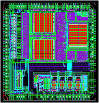
ATLAS HCCStar
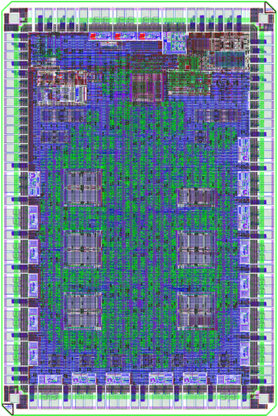
This 3.5 x 5.2 mm chip was fabricated in a 130 nm CMOS technology
after being synthesized, and assembled using Cadence design tools.
Extensive verification was carried out using Cadence's Verilog
simulator at the RTL, post-synthesis, and post-PNR (with full
back-annotation) levels. The analog blocks were simulated using
Cadence's analog simulator. This nearly all digital chip is the
controller and data flow manager for the front-end electronics in the
ATLAS silicon strip upgrade project (ITk Strips).
ATLAS AMAC
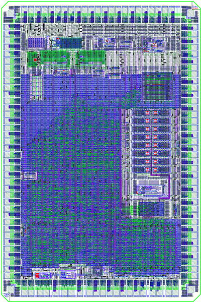
This 3.5 x 5.2 mm chip was fabricated in a 130 nm CMOS technology. It
is a mixed analog/digital chip that provides autonomous analog
measurement and control functionality. The analog blocks were
designed and verified using Cadence's schematic, layout, and
simulation tools. The digital design was synthesized and the entire
chip assembled using Cadence's tools. Extensive verification was
carried out using Cadence's Verilog simulator at the RTL,
post-synthesis, and post-PNR (with full back-annotation) levels.
Some older examples of Penn contributions to the ATLAS project - designs made using the Cadence tools in analog IC, digital IC, and board design and verification are:
ATLAS ASDBLR
This 3.2 x 3.3 mm chip was fabricated in a radiation hard bipolar silicon on insulator technology after being hand crafted in the Cadence layout tool and simulated in a third party analog simulator.
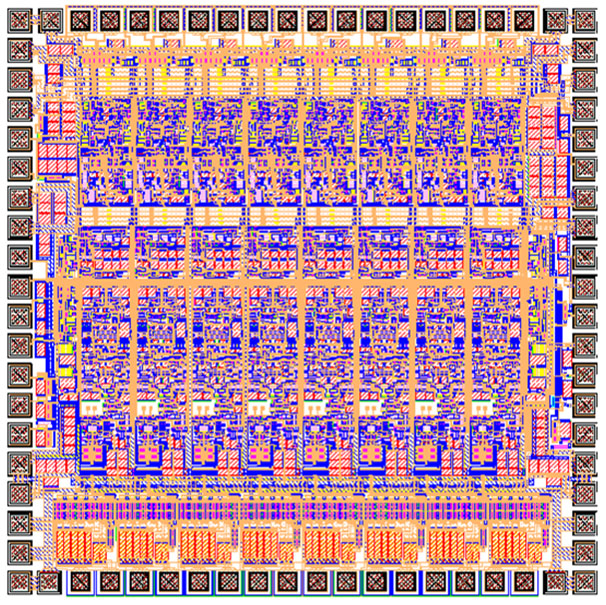
ATLAS DTMROC
This 5 x 5.2 mm chip was fabricated in a 0.25 micron CMOS technology after being synthesized , assembled, and then simulated (in both Verilog and analog simulators) using a mixture of Cadence and third party tools.
Barrel AR1FL
This 10 cm, 14 layer, four blind, one through, via board with 0.004" design rules, mounting 30 fine pitch ball grid array packages on two sides is able to sense fC signals on one side while operating 40 MHz digital devices on the other. The DTMROC chips are mounted on this side, the ASDBLR chips are on the other side of the board - this particular design (one of twelve slightly different configurations) handles 176 channels for dual threshold wire drift chamber with up to 20MHz hit rate, 1ns time measurement, and a 6 microsecond L1 pipeline.
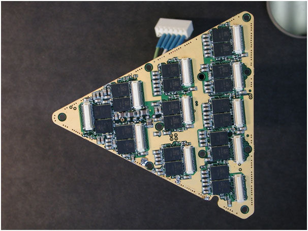
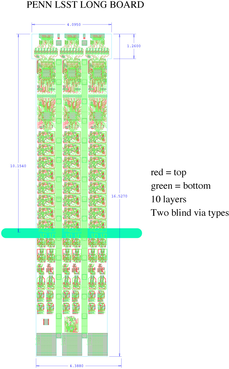
LSST was the highest ranked ground based astronomy project in the recent National Academy of Sciences / National Research Council decadal survey report "New Worlds New Horizons" . The project received Department of Energy CD1 approval at the end of 2011 and is now proceeding apace. This new 8.4 m telescope is designed to carry the largest array of astronomical CCD sensors ever and Penn is responsible for designing and testing the extremely dense printed circuit board that mounts two custom ASICs developed in Paris. The technical requirements include a six electron noise floor, a 10,000::1 cross talk rejection, operating at – 100 K, and fitting 3,000 channels of front end in a 65 cm diameter space. The very high density also implies very low power. The electronics package is more than an order of magnitude lower power and almost two orders of magnitude more compact than any other major astronomical instrument.
The SNO+ experiment is the successor to the very successful Sudbury Neutrino Observatory (SNO). While SNO was aimed at solving the long-standing solar neutrino problem, SNO+ is aimed at another very important question, determining whether the neutrino is its own antiparticle.
The University of Pennsylvania group designed, laid out, and built all the electronics for SNO using the CADENCE tools. Important upgrades were needed for SNO+ to accomodate much higher data rates, and two critical new boards were designed and built by graduate students. A new communications board, called the XL3, was created by students Richie Bonventre and Tim
Shokair. This board acts as a `translator' from TCP/IP protocol to the proprietary "SNOBUS" protocol use by the SNO/SNO+ electronics. The improvements made by Bonventre and Shokair over the old system have increased the data throughput by over a factor of 100. A second board, called the MTC/A+, was designed, laid out, and built by student Andy Mastbaum. The MTC/A+ serves as a central analog summing node for the trigger signals from the approximately 10,000 channels of the front-end electronics. In addition to summing these signals while maintaining a dynamic range of nearly three orders of magnitude, the MTC/A+ includes logic that can be programmed to have the detector "retrigger" automatically to catch important low-energy backgrounds, as well as
significantly reducing deadtime that was part of the original SNO design. A third board, the TUB II, is now in the design phase, and we expect to get a new student who would use the CADENCE tools to develop this board and lay it out, hopefully for production a year from now.
This page maintained by Paul Keener (keener@hep.upenn.edu) and Mike Reilly (mbreilly@hep.upenn.edu) - last edited Oct 2024
*Cadence is a trademark of Cadence Design Systems, Inc., 2655 Seely Avenue, San Jose, CA 95134.

