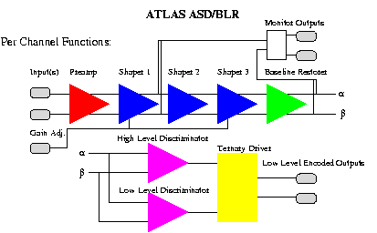
The ASDBLR is a custom integrated circuit that
provides the complete analog signal processing chain (amplification, shaping, baseline restoration, and discrimination)
for the ATLAS TRT straw sensors. It includes eight identical channels per chip.
The ASIC is implemented in bipolar technology although some FET's have migrated into the design. Prototypes have been tested in both the MAXIM and DMILL processes, several
complete prototypes and a "pre-production"
version have been submitted to the DMILL process.
Amplifier/Shaper/Discriminator with Baseline Restoration Peaking Time 7 - 8 nsec Selectable Shaping Circuit: Xenon gas mixture or "typical" fast gas Two Discriminators - TR photons 6 KeV, Tracking 200 eV Three State (Ternary) Low Level Differential Outputs Power Dissipation ~ 35 mW Radiation Hard ~ > 3 MRads Ionizing Radiation and ~ 1X10^14 Neutrons/cm^2
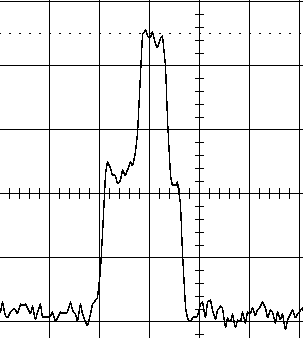
Output of the Ternary Receiver. The first transition
shows that the input signal exceeded the tracking threshold.
The second, higher transition, indicates that the ,
Transition Radiation threshold was triggered as well.
Recent Work/Reports (PRR stuff)
Input Protection
The requirement for a tight layout and a very robust input protection (0.5mJ) led to the development of a custom input protection network that has been included in the ASDBLR00. We will be evaluating carefully the benefit of this network due to its high overhead: Silicon area (Total Area ~.4mm X 3mm) Parasitic capacitance (5pF.) and additinal resistance (~15 ohms). The Structure can be scaled easily, It is designed as 5 independent parallel devices.Layout of Input Protection Circuit Yield of ASDBLR99 Ceramic QFP ASDBLR00 3fC Threshold Deviations from Chip average for 15 of 18 tested chips. August 2001 Theat 3fC is histogrammed in units of equivalent input charge, fC. RMS = 0.1fC
ASDBLR01 - Yield and Input protection Results from Studies of ASDBLR 99, 00, 01. Updated March 21, 2002 - - The ASDBLR01 is a refabrication of the ASDBLR00 with metal (connnection) only changes to the input protection. Pinout and all functionality remains the same. This ASIC exibits similar intrinsic noise to the ASDBLR99 and has several variations of the input protection structure. It is clear that external protection diodes will be required for production parts, but that the chip can be designed to withstand .6mJ input discharges, a factor of two larger than the protection on the ASDBLR99.Test Amp for CERN studies. An ASDBLR01 is mounted in a box and two channels are available for studies of its analog properties. This note describes the Test Amp and measurements made with it at Penn (March 02)
Reports, Documents, Presentations &PRR Much of the documentation used to prepare the Production Readiness Review can be found here.ASDBLR_00 Bonding Diagrams
Bonding Diagram for ASDBLR_00 in TQFP package Front of ASDBLR ASIC for input identification. ASDBLR_00 in 64 Lead Ceramic Quad package
ASDBLR_00 FBGA Package design
We are investigating several packaging options for ASDBLR's including full custom Fine Pitch Ball Grid Arrays. The design below is compact enough to allow two eight channel ASDBLR chips to be placed side by side on a 16X20mm printed circuit board.Proposed 7.2mm X 9mm FBGA substrate design. Zoomed in on top layer of FBGA substrate layout. ASDBLR00 FBGA Ball Footprint and Mechanical Information . ASDBLR00 FBGA Bonding Diagram . ASDBLR00 FBGA Die Orientation. Ball to Signal Mapping (valid for ASDBLR 00' or 02').
ASDBLR_02 Production Version March 2002
Pad Allocation and Signal Specification of ASDBLR02 Report on Production testing September 04 6" WAFER ARRAY of ASDBLR02 1042 Die Pad #1 Location and Die Orientation on Wafer Pad Frame of ASDBLR02 FBGA Bonding Diagram for ASDBLR02 Ball to Signal Mapping (valid for ASDBLR 00' or 02'). 64 Lead TQFP Bonding Diagram for ASDBLR02
Channel Response Simulations ASDBLR02 Last Change January 7 , 2004